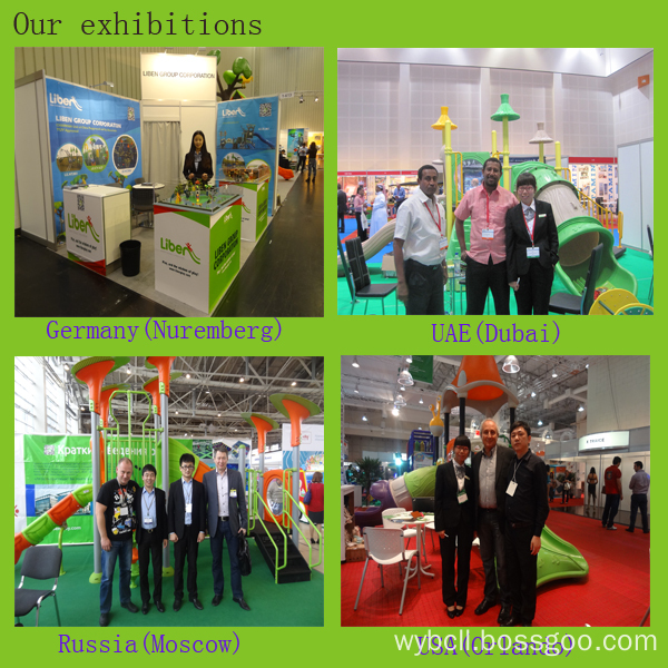
How to make a printed circuit board
Printed circuit boards are a big part of electronics production, and they are also the technologies that best represent the level of electronics enthusiasts. Printed circuit boards are referred to as printed boards for short, and factory production is very different from amateur production. The factory generally designs the printed board diagram according to the circuit schematic provided by the customer, and then makes the printed board through photolithography and other techniques, and then forms the finished product by soldering, printing, etc., and requires a series of equipment.
In the traditional amateur production, printed boards can only be produced using a copper-plated and corrosive solution. In recent years, new types of technologies such as universal test boards and photosensitive circuit boards have been introduced to liberate vast numbers of electronics enthusiasts and electronic product developers. In addition to the popularity of PCs, designing circuits with CAD software and automatically generating PCBs (printed circuit boards) are not difficult. It is even more convenient to print on the film directly with the photosensitive circuit board.
Bitbaby learned ORCAD software in the school curriculum and used it to design a typical application circuit for the 8031 ​​microcontroller. It feels really good. The teacher is also not allowed to use ORCAD's automatic routing function. The figure of Bitbaby's manual wiring can be beautiful, and the corners of the traces are smooth transitions. Taking full account of this design makes the printing plate stronger, so that the teacher thinks that the wiring is automatic. It (not blowing :-). Unfortunately, no printer printed out the PCB at that time.
PROTEL is known to most electronic enthusiasts, but unfortunately Bitbaby has not studied it deeply. General electronic production circuit is not complicated, for the veteran, as long as you can use the brain to design a printed circuit board diagram, so talk about the traditional production method of printed board.
First, design the printed circuit board diagram on the basis of the circuit schematic diagram on the paper, the correct connection among each component is important, but also pay attention to the size of the components, arrangement position, interference and so on. (Bitbaby will later write a special article on how to design the printed board.) After the design is completed, the schematics should be re-checked, and the components should be placed in their respective positions to adjust the hole spacing and alignment. Pay attention to the positive and negative, and sometimes accidentally design the opposite side. You can write the original image on carbon paper once. Then you have what you need on the back of the paper.
Bitbaby's method of making a printed circuit board is to cut out the designed 1:1 drawing, attach it to the copper surface of the single-faced copper-clad board with transparent glue, and then punch it in the place where the hole is drilled to form a recess. The pit, so that drilling with a small electric drill will not slip. Then use a self-made small electric drill (recording machine motor modification) to drill holes, tear off the drawings after all finishes, and paint directly with a brush.
Since holes are already positioned, it is not difficult to draw, just remember that the holes are connected together. Generally uncomplicated circuits use this method to make the circuit board extremely fast (even if the copying paper is saved :-). If the complicated circuit can insert a copy of carbon paper between the drawing and the copper-clad board, then the printed circuit board drawing will be described again. Place the hole deeper, and then use a brush to paint the line.
If there is no paint, trace lines can be traced with a better quality marker, or traced with a correction fluid, but the circuit board for correcting the fluid profile is not very beautiful, and the width of the circuit needs to be corrected after drying. Nail polish can also be used, dried faster and easier to use than correction fluid. During the tracing, pay attention to the distance between the lines, and surround the holes to form a circle to facilitate welding.
It takes a long time for the paint to dry. After the paint is dry, it can be put into the corrosive solution. The corrosive solution is generally made of ferric chloride and water. The ferric chloride is a yellowish solid and it is easy to absorb the moisture in the air. So Should be sealed and stored. When ferric chloride solution is used, 40% of ferric chloride and 60% of water are generally used. Of course, more ferric chloride is used, or warm water (not hot water to prevent paint shedding) can make the reaction faster. .
Note that ferric chloride has a certain degree of corrosivity and it is best not to get it on the skin or clothes (difficult to wash :-( reaction containers with cheap plastic basins, just like the circuit board. Corrosion is from the edge In the beginning, when the unpainted copper foil is corroded, the circuit board should be taken out in time to prevent the paint from falling off and eroding the useful circuit.
Rinse with clean water at this time, and scrape off the paint with bamboo or other materials (the paint comes out of the liquid and is easier to remove). If it is not easy to scratch, just use hot water. Then wipe dry and polish it with sandpaper to reveal shiny copper foil. A printed circuit board is ready. In order to preserve the results, Bitbaby usually coats the polished circuit board with rosin solution, which can both help the solder and prevent oxidation.
| Measurements (m) | can be customized |
| Certificate |
ISO14001, ISO18000, ISO9001 Certificate,
and GS certificate from TUV Company of Germany.
|
| Color | Various, according to your requirements |
| Materials |
A. Plastic parts: Imported LLDPE E. Outer cover: Soft Covering PVC
(Different material is available according to your needs)
|
| Advantage |
a.Anti-UV
b.Anti-static
c.Security
d.Environmental protection e.Uneasy to lose shape |
| Function |
1.Can protect children safe when they playing indoor, and let they enjoy the play freely 2.Suitable for improving Children energy and imagination 3.Helping them grow up happily, cleverly, and healthily |
| Installation | Professional CAD instruction, assembly procedure and project case . |
| Age Range | Children |
| Apply to | Amusement park, gymnasium, Kindergarten, Preschool, etc. |
| Packing | Standard export packing |
| Remark |
We can design and produce as your requirements |
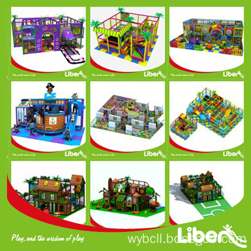
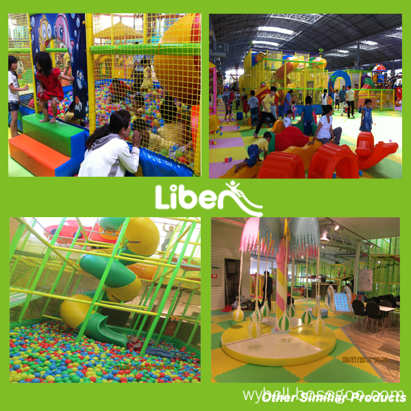
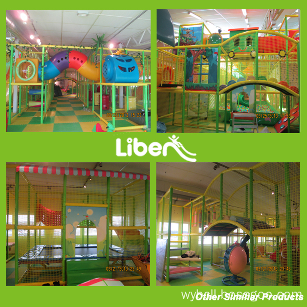
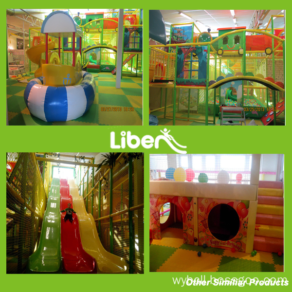
Indoor Playset, Indoor Playset for Kids, Plastic Slides, Plastic Playhouse, Soft Play
Liben Group Corporation , http://www.indoortrampoline.de